CircuitWalaCircuitWalaCircuitWalaCircuitWala
  • Our Company
    • About CircuitWala
    • Why to Choose CircuitWala?
    • Industries We Serve
    • Privacy Policy
  • Products
    • Single Layer PCB
    • Double Layer PCB
    • Multi Layer PCB
    • Metal PCB
    • Flexible PCB
  • Services
    • PCB Manufacturing
    • PCB Layout
    • PCB Assembly
  • Manufacturing
    • Technical Capabilities
    • PCB Glossary
    • Quality Control
  • Blog
  • Contact Us
  • Login
Want create site? Find Free WordPress Themes and plugins.

Metal PCB

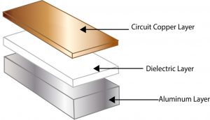
There are many terms for this category of PCBs; Aluminum Clad, Aluminum Base, Metal Clad Printed Circuit Board (MCPCB), Insulated Metal Substrate (IMS or IMPCB), Thermally Conductive PCBs, etc. but they all mean the same thing and perform the identical way.

Benefits of Metal PCBs

  • Intensely Higher Heat Dissipation (superior to standard FR-4 constructions)
  • More Conductive Dielectrics with Reduced Width (typically 5 to 10 times as thermally conductive as conventional epoxy-glass and a tenth of the thickness)
  • Exponentially Efficient in Thermal Transfer (more capable than a conventional rigid PCB)
  • Competent to Use Low Weight Copper Layer (able to use lower copper weights than suggested by the IPC Heat-rise charts)
Sr Specifications Standard
1. Minimum conductor width 6 mils( 0.15 mm)
2. Minimum conductor Spacing/Air gap 6 mils( 0.15 mm)
3. Minimum Plated hole size 16 mils( 0.4mm)
4. Maximum Plated hole size 240 mils( 6mm)
5. Maximum board size 300 mm x 350 mm
6. Maximum number of layers 2
7. Minimum copper thickness 1 Oz (35 microns)
8. Maximum copper thickness 3 Oz (105 microns)
9. Dedicated Electrical Testing (BBT) Available
10. PCB Cutting options Maximum copper thickness

Product Finish

Sr Specifications Standard
1. Single Sided HAL, Lacquer
2. Double Sided HHAL, TIN , Electroplated Gold & Nickel
3. Solder Mask Finish PISM, Liquid Solder Mask
4. Solder Mask color Green, White, Black, Blue ,Red
5. Legend/Ident color White, Black, yellow, Green
6. Special Requirement Carbon Printing on Push Button , Selective Gold & Nickel plating on Connecting Tabs

Product Raw Material

Sr Specifications Standard
1. Single Side FR1,FR4, CEM1,CEM3, PP, Metal Clad
2. Double Side FR4
2. Board Thickness (in mm) 0.4 , 0.8 ,1.0 , 1.2, 1.6 ,2.4 , 3.2
Did you find apk for android? You can find new Free Android Games and apps.

Our Company

  • About CircuitWala
  • Why to Choose CircuitWala?
  • Industries We Serve
  • Contact Us

Services

  • PCB Manufacturing
  • PCB Assembly
  • PCB Layout

Products

  • Single Layer PCB
  • Double Layer PCB
  • Metal PCB
  • Multi Layer PCB
  • Flexible PCB

Technoology

  • Technical Capabilities
  • PCB Glossary
  • Quality Control
© 2017 CircuitWala
 +91 99 796 333 44      [email protected]
  • Our Company
    • About CircuitWala
    • Why to Choose CircuitWala?
    • Industries We Serve
    • Privacy Policy
  • Products
    • Single Layer PCB
    • Double Layer PCB
    • Multi Layer PCB
    • Metal PCB
    • Flexible PCB
  • Services
    • PCB Manufacturing
    • PCB Layout
    • PCB Assembly
  • Manufacturing
    • Technical Capabilities
    • PCB Glossary
    • Quality Control
  • Blog
  • Contact Us
  • Login
CircuitWala